ICGOO在线商城 > IPA037N08N3 G

 Datasheet下载
- 型号: IPA037N08N3 G
- 制造商: Infineon
- 库位|库存: xxxx|xxxx
- 要求:
| 数量阶梯 | 香港交货 | 国内含税 |
| +xxxx | $xxxx | ¥xxxx |
查看当月历史价格
查看今年历史价格
IPA037N08N3 G产品简介:
ICGOO电子元器件商城为您提供IPA037N08N3 G由Infineon设计生产,在icgoo商城现货销售,并且可以通过原厂、代理商等渠道进行代购。 提供IPA037N08N3 G价格参考以及InfineonIPA037N08N3 G封装/规格参数等产品信息。 你可以下载IPA037N08N3 G参考资料、Datasheet数据手册功能说明书, 资料中有IPA037N08N3 G详细功能的应用电路图电压和使用方法及教程。
| 参数 | 数值 |
| 产品目录 | |
| ChannelMode | Enhancement |
| 描述 | MOSFET N-CH 80V 75A TO220-3MOSFET N-KANAL POWER MOS |
| 产品分类 | FET - 单分离式半导体 |
| FET功能 | 标准 |
| FET类型 | MOSFET N 通道,金属氧化物 |
| Id-ContinuousDrainCurrent | 75 A |
| Id-连续漏极电流 | 75 A |
| 品牌 | Infineon Technologies |
| 产品手册 | |
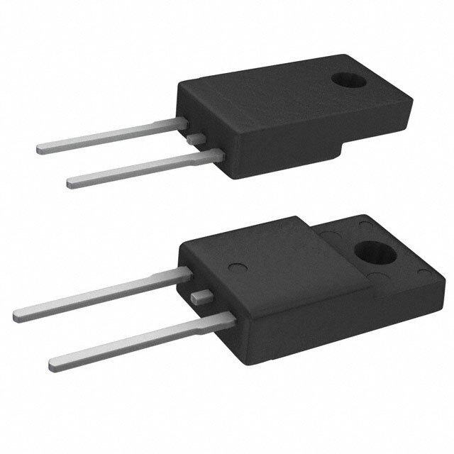
| 产品图片 |
|
| rohs | 符合RoHS无铅 / 符合限制有害物质指令(RoHS)规范要求 |
| 产品系列 | 晶体管,MOSFET,Infineon Technologies IPA037N08N3 GOptiMOS™ |
| 数据手册 | http://www.infineon.com/dgdl/IPA037N08N3_Rev2.0.pdf?folderId=db3a304313b8b5a60113cee8763b02d7&fileId=db3a30431d8a6b3c011dce12d2e1353d |
| 产品型号 | IPA037N08N3 G |
| Pd-PowerDissipation | 41 W |
| Pd-功率耗散 | 41 W |
| Qg-GateCharge | 29 nC |
| Qg-栅极电荷 | 29 nC |
| RdsOn-Drain-SourceResistance | 3.7 mOhms |
| RdsOn-漏源导通电阻 | 3.7 mOhms |
| Vds-Drain-SourceBreakdownVoltage | 80 V |
| Vds-漏源极击穿电压 | 80 V |
| Vgs-Gate-SourceBreakdownVoltage | +/- 20 V |
| Vgs-栅源极击穿电压 | 20 V |
| 上升时间 | 49 ns |
| 下降时间 | 13 ns |
| 不同Id时的Vgs(th)(最大值) | 3.5V @ 155µA |
| 不同Vds时的输入电容(Ciss) | 8110pF @ 40V |
| 不同Vgs时的栅极电荷(Qg) | 117nC @ 10V |
| 不同 Id、Vgs时的 RdsOn(最大值) | 3.7 毫欧 @ 75A,10V |
| 产品种类 | MOSFET |
| 供应商器件封装 | PG-TO220-FP |
| 其它名称 | IPA037N08N3G |
| 典型关闭延迟时间 | 46 ns |
| 功率-最大值 | 41W |
| 包装 | 管件 |
| 商标 | Infineon Technologies |
| 商标名 | OptiMOS |
| 安装类型 | 通孔 |
| 安装风格 | Through Hole |
| 封装 | Tube |
| 封装/外壳 | TO-220-3 整包 |
| 封装/箱体 | TO-220FP-3 |
| 工厂包装数量 | 500 |
| 晶体管极性 | N-Channel |
| 最大工作温度 | + 175 C |
| 最小工作温度 | - 55 C |
| 标准包装 | 500 |
| 漏源极电压(Vdss) | 80V |
| 电流-连续漏极(Id)(25°C时) | 75A (Tc) |
| 系列 | IPA037N08 |
| 通道模式 | Enhancement |
| 配置 | Single |
| 零件号别名 | IPA037N08N3GXKSA1 SP000446772 |


.jpg)


PDF Datasheet 数据手册内容提取
IPA037N08N3 G OptiMOS(TM)3 Power-Transistor Product Summary Features V 80 V DS • Ideal for high frequency switching and sync. rec. R 3.7 mW DS(on),max • Optimized technology for DC/DC converters I 75 A D • Excellent gate charge x R product (FOM) DS(on) • Very low on-resistance R DS(on) • N-channel, normal level • 100% avalanche tested • Pb-free plating; RoHS compliant • Qualified according to JEDEC1) for target applications • Halogen-free according to IEC61249-2-21 Type IPA037N08N3 G Package PG-TO220-FP Marking 037N08N Maximum ratings, at T =25 °C, unless otherwise specified j Parameter Symbol Conditions Value Unit Continuous drain current I T =25 °C2) 75 A D C T =100 °C 54 C Pulsed drain current3) ID,pulse TC=25 °C 300 Avalanche energy, single pulse4) EAS ID=75 A, RGS=25 W 680 mJ Gate source voltage V ±20 V GS Power dissipation P T =25 °C 41 W tot C Operating and storage temperature T , T -55 ... 175 °C j stg IEC climatic category; DIN IEC 68-1 55/175/56 1)J-STD20 and JESD22 2) Current is limited by package; with an RthJC=0.7 K/W in a standard TO-220 package the chip is able to carry 178A. 3) See figure 3 for more detailed information 4) See figure 13 for more detailed information Rev. 2.1 page 1 2013-08-27
IPA037N08N3 G Parameter Symbol Conditions Values Unit min. typ. max. Thermal characteristics Thermal resistance, junction - case R - - 3.7 K/W thJC Electrical characteristics, at T =25 °C, unless otherwise specified j Static characteristics Drain-source breakdown voltage V V =0 V, I =1 mA 80 - - V (BR)DSS GS D Gate threshold voltage V V =V , I =155 µA 2 2.8 3.5 GS(th) DS GS D V =80 V, V =0 V, Zero gate voltage drain current I DS GS - 0.1 1 µA DSS T =25 °C j V =80 V, V =0 V, DS GS - 10 100 T =125 °C j Gate-source leakage current I V =20 V, V =0 V - 1 100 nA GSS GS DS Drain-source on-state resistance R V =10 V, I =75 A - 3.2 3.7 mW DS(on) GS D V =6 V, I =38 A - 3.9 6.2 GS D Gate resistance R - 1.9 - W G |V |>2|I |R , Transconductance g DS D DS(on)max 66 132 - S fs I =75 A D Rev. 2.1 page 2 2013-08-27
IPA037N08N3 G Parameter Symbol Conditions Values Unit min. typ. max. Dynamic characteristics Input capacitance C - 6100 8110 pF iss V =0 V, V =40 V, Output capacitance C GS DS - 1640 2180 oss f=1 MHz Reverse transfer capacitance C - 59 - rss Turn-on delay time t - 23 - ns d(on) Rise time tr V =40 V, V =10 V, - 49 - DD GS I =75 A, R =1.6 W Turn-off delay time t D G,ext - 46 - d(off) Fall time t - 13 - f Gate Charge Characteristics5) Gate to source charge Q - 29 - nC gs Gate to drain charge Q - 17 - gd V =40 V, I =75 A, Switching charge Q DD D - 30 - sw V =0 to 10 V GS Gate charge total Q - 88 117 g Gate plateau voltage V - 4.8 - V plateau Output charge Q V =40 V, V =0 V - 119 158 nC oss DD GS Reverse Diode Diode continous forward current I - - 75 A S T =25 °C C Diode pulse current I - - 300 S,pulse V =0 V, I =75 A, Diode forward voltage V GS F - 1.0 1.2 V SD T =25 °C j Reverse recovery time trr V =40 V, I =I , - 62 - ns R F S di /dt=100 A/µs Reverse recovery charge Q F - 130 - nC rr 5) See figure 16 for gate charge parameter definition Rev. 2.1 page 3 2013-08-27
IPA037N08N3 G 1 Power dissipation 2 Drain current P =f(T ) I =f(T ); V ≥10 V tot C D C GS 50 80 40 60 30 P [W] tot I [A] D 40 20 20 10 0 0 0 50 100 150 200 0 50 100 150 200 T [°C] T [°C] C C 3 Safe operating area 4 Max. transient thermal impedance I =f(V ); T =25 °C; D=0 Z =f(t ) D DS C thJC p parameter: t parameter: D=t /T p p 103 101 limited by on-state 1 µs resistance 10 µs 0.5 102 100 µs 100 0.2 1 ms W] A] K/ 0.1 [D 10 ms [C I hJ 0.05 Zt 101 DC 10-1 0.02 0.01 single pulse 100 10-2 10-1 100 101 102 10-5 10-4 10-3 10-2 10-1 100 101 V [V] t [s] DS p Rev. 2.1 page 4 2013-08-27
IPA037N08N3 G 5 Typ. output characteristics 6 Typ. drain-source on resistance I =f(V ); T =25 °C R =f(I ); T =25 °C D DS j DS(on) D j parameter: V parameter: V GS GS 300 10 10 V 7 V 6 V 4.5 V 5 V 5.5 V 6 V 250 8 200 5.5 V ] 6 W m [A] D 150 [on) I S( D R 4 7 V 100 5 V 10 V 2 50 4.5 V 0 0 0 1 2 3 4 5 0 50 100 150 200 250 300 V [V] I [A] DS D 7 Typ. transfer characteristics 8 Typ. forward transconductance I =f(V ); |V |>2|I |R g =f(I ); T =25 °C D GS DS D DS(on)max fs D j parameter: T j 300 200 250 150 200 I [A] D 150 g [S] fs 100 100 50 50 175 °C 25 °C 0 0 0 2 4 6 8 0 50 100 150 V [V] I [A] GS D Rev. 2.1 page 5 2013-08-27
IPA037N08N3 G 9 Drain-source on-state resistance 10 Typ. gate threshold voltage R =f(T ); I =75 A; V =10 V V =f(T ); V =V DS(on) j D GS GS(th) j GS DS parameter: I D 8 4 3.5 6 3 1550 µA ] 2.5 155 µA W m max V] [n) 4 [h) 2 DS(o typ GS(t R V 1.5 2 1 0.5 0 0 -60 -20 20 60 100 140 180 -60 -20 20 60 100 140 180 T [°C] T [°C] j j 11 Typ. capacitances 12 Forward characteristics of reverse diode C=f(V ); V =0 V; f=1 MHz I =f(V ) DS GS F SD parameter: T j 104 103 Ciss Coss 175 °C, max 103 102 25 °C 175 °C F] A] p C [ I [F Crss 25 °C, max 102 101 101 100 0 20 40 60 80 0 0.5 1 1.5 2 V [V] V [V] DS SD Rev. 2.1 page 6 2013-08-27
IPA037N08N3 G 13 Avalanche characteristics 14 Typ. gate charge I =f(t ); R =25 W V =f(Q ); I =75 A pulsed AS AV GS GS gate D parameter: T parameter: V j(start) DD 1000 12 40 V 10 20 V 60 V 100 8 A] 150 °C 100 °C 25 °C V] [AV [GS 6 I V 10 4 2 1 0 0.1 1 10 100 1000 0 20 40 60 80 100 t [µs] Q [nC] AV gate 15 Drain-source breakdown voltage 16 Gate charge waveforms V =f(T ); I =1 mA BR(DSS) j D 90 V GS Q g 80 V] [S) S D R( B V Vgs(th) 70 Qg(th) Qsw Qgate Q Q 60 gs gd -60 -20 20 60 100 140 180 T [°C] j Rev. 2.1 page 7 2013-08-27
IPA037N08N3 G PG-TO-220-3-31 Rev. 2.1 page 8 2013-08-27
IPA037N08N3 G Published by Infineon Technologies AG 81726 Munich, Germany © 2008 Infineon Technologies AG All Rights Reserved. Legal Disclaimer The information given in this document shall in no event be regarded as a guarantee of conditions or characteristics. With respect to any examples or hints given herein, any typical values stated herein and/or any information regarding the application of the device, Infineon Technologies hereby disclaims any and all warranties and liabilities of any kind, including without limitation, warranties of non-infringement of intellectual property rights of any third party. Information For further information on technology, delivery terms and conditions and prices, please contact the nearest Infineon Technologies Office (www.infineon.com). Warnings Due to technical requirements, components may contain dangerous substances. For information on the types in question, please contact the nearest Infineon Technologies Office. Infineon Technologies components may be used in life-support devices or systems only with the express written approval of Infineon Technologies, if a failure of such components can reasonably be expected to cause the failure of that life-support device or system or to affect the safety or effectiveness of that device or system. Life support devices or systems are intended to be implanted in the human body or to support and/or maintain and sustain and/or protect human life. If they fail, it is reasonable to assume that the health of the user or other persons may be endangered. Rev. 2.1 page 9 2013-08-27
Mouser Electronics Authorized Distributor Click to View Pricing, Inventory, Delivery & Lifecycle Information: I nfineon: IPA037N08N3 G